Description:
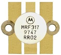
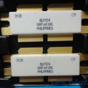
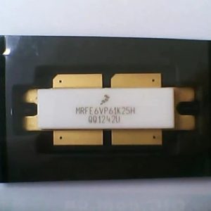
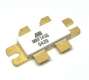
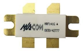
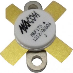
Designed primarily for wideband largesignal output amplifier stages in 30200 MHz frequency range. Guaranteed Performance at 150 MHz, 28 Vdc Output Power 100 W Minimum Gain = 9.0 dB BuiltIn Matching Network for Broadband Operation 100% Tested for Load Mismatch at all Phase Angles with 30:1 VSWR Gold Metallization System for High Reliability High Output Saturation Power Ideally Suited for Carrier/120 W Peak AM Amplifier Service Guaranteed Performance in Broadband Test Fixture MAXIMUM RATINGS
Rating CollectorEmitter Voltage CollectorBase Voltage EmitterBase Voltage Collector Current Continuous Collector Current Peak (10 seconds) Total Device Dissipation 25°C (1) Derate above 25°C Storage Temperature Range Symbol VCEO VCBO VEBO IC PD Tstg Value to +150 Unit Vdc Adc Watts W/°C °C
Characteristic Thermal Resistance, Junction to Case Symbol RJC Max 0.65 Unit °C/W
Specifications:
●Product Attribute Attribute Value Search Similar
●Product Category: RF Bipolar Transistors
●Product Type: RF Bipolar Transistors
●Subcategory: Transistors
Features:
●ELECTRICAL CHARACTERISTICS : (TC = 25°C unless otherwise noted.)
●CommonEmitter Amplifier Power Gain: (VCC = 28 Vdc, Pout = 150 MHz, IC (Max) = 6.5 Adc)
●Collector Efficiency :(VCC = 28 Vdc, Pout = 150 MHz, IC (Max) = 6.5 Adc) Load Mismatch (VCC = 28 Vdc, Pout 100 W CW, = 150 MHz, VSWR = 30:1 all phase angles)
●GPE No Degradation in Output Power dB %



Reviews
There are no reviews yet.