
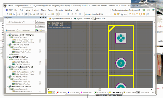
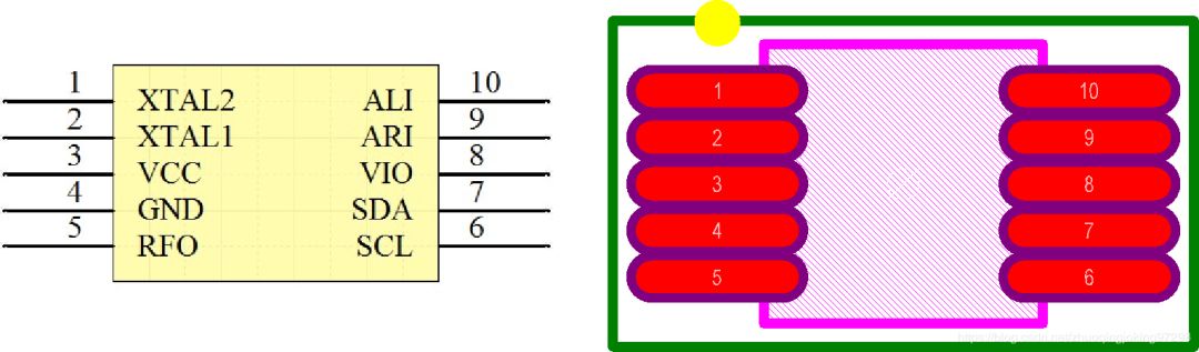
- Schematic and PCB package
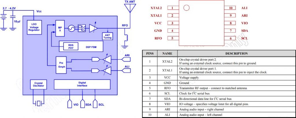
First, according to the data sheet of QN8027, find the main parameters of the chip and the schematic diagram of the reference design. Lay the foundation for the subsequent production of the test circuit board.
In the data sheet of the QN8027, the mathematical description of the two-channel signal of the two inputs being processed by the MPX circuit is described:
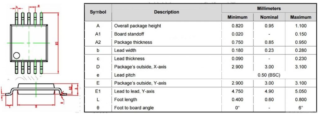
According to the package information in the QN8027 data sheet, the chip package is 10-Lead Plastic Package, and the correct corresponding IC package device is added in AtiumDesign. Among the most critical parameters:
Pin spacing e: 0.5mm;
Pin width b: 0.25mm;
End-to-end distance between double-row pins: E1 : 4.9mm
Reference Schematic and Experiment Board Design
The following is the reference design circuit found in the documentation of QN8027 that others involved in Baidu’s collection. It shows the parameters of some basic components around the chip:
Crystal frequency 12Mhz
Load inductance of RFO: 150nH
Audio input coupling capacitor: 4.7uF
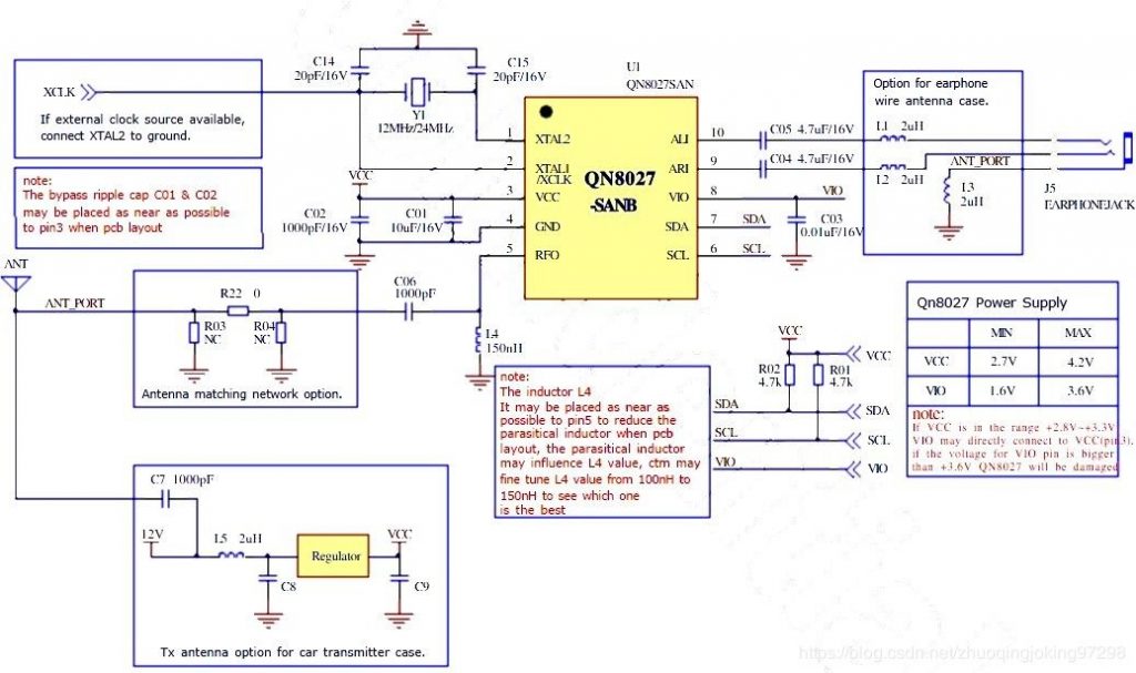
According to the reference circuit diagram, the design has a six-pin interface, which can be directly inserted into the breadboard and can be connected to the previous test circuit board with the I2C bus microcontroller experimental circuit board.
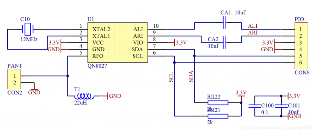
The basic schematic diagram of the experimental circuit board is given below.
Four small experimental circuit boards were obtained by direct rapid thermal transfer plate making.
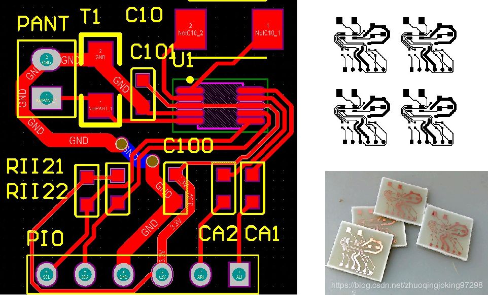
Formed Experiment Board
After an hour or so of design and fabrication, the breadboard is now ready to be tested.
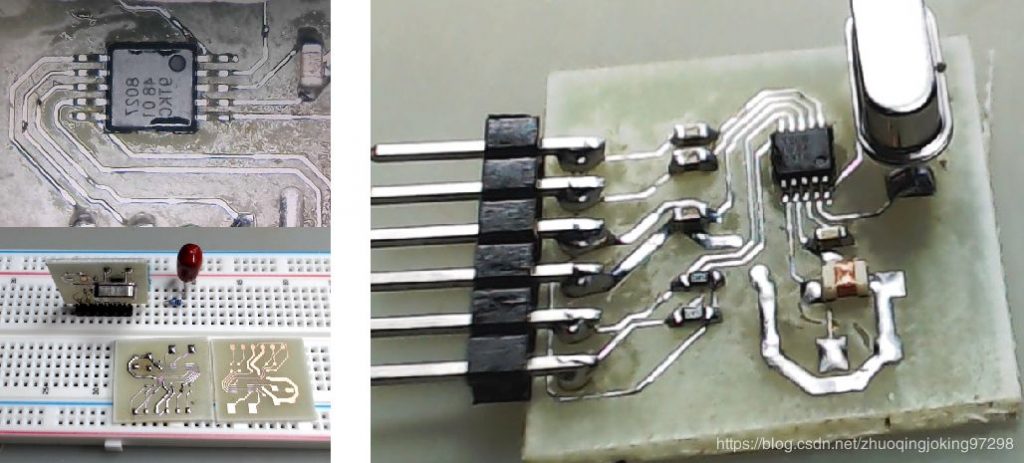
After the production is completed, the rest is to carry out software design and performance testing. Let’s save this part until the afternoon. The test results support the sound beacon scheme in the competition rules to be finalized tomorrow.


