
Description
With the proliferation of wireless devices, strong signal strength and high-quality RF antenna design and integration are now required for optimal performance. Whether it is an off-the-shelf product or a highly customized solution, antenna integration is not trivial, nor should it be an afterthought. The antenna input impedance must be matched to 50Ω to ensure maximum power transfer from the RF circuit to the antenna without any reflections.
Key Implementation Aspects of RF Antennas
One of the most critical factors in implementing a trace or chip antenna is the impedance matching of the antenna to the radio chip. Antennas must be impedance matched when assembled in a product, as antenna mismatch can lead to the following consequences:
Reduced range loss: Impedance mismatches cause more signal reflections, which provide less power for the antenna to radiate into free air, reducing range
Reduce the return loss of the antenna at the specific desired operating frequency: At the desired operating frequency, the antenna should have a return loss of at least -10 dB or less. Impedance mismatch increases return loss in the desired frequency range, resulting in reduced RF power delivered to the antenna in that frequency range
Higher power consumption: The antenna radiates less power due to signal reflections caused by impedance mismatch. This will require the RF chip to transmit the signal at greater power to achieve the desired range, increasing overall power consumption
RF chip heating due to signal reflection: Signal reflection due to impedance mismatch causes RF energy to flow back into the transmitter, causing the transmitter to heat up, thereby extending the life of the transmitter
Unreliable data throughput: High packet error rate (PER) due to impedance mismatch, signal reflection and data throughput of RF transceiver may not be optimal for this product
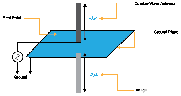
Most PCB trace or chip antennas are constructed as quarter-wave monopoles, which require a solid ground plane on all PCB layers to function properly. This ground plane is called “parallel” and is important because it acts as a dummy pole for the monopole antenna, allowing it to function like a full dipole antenna.

The balanced length and width should be at least λ/4 units. The figure below shows the effect of various ground plane sizes using a chip antenna implementation example.

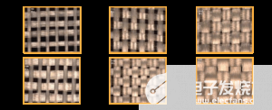
In addition, the PCB material also affects the antenna system impedance. Especially for FR4-type substrates, which also depend on the weave pattern, resulting in changes in the dielectric constant of the material depending on the tightness of the weave, and possible local impedance discontinuities due to changes in parasitic capacitance. For the implementation of PCB trace antennas, designers must strictly follow the antenna design guidelines and antenna manufacturer’s recommendations on trace width, layer stack, balance size, PCB material, and material weave pattern, so that when implementing a trace or chip antenna for best results. Antenna system impedance is also affected by other circuit components around it and product housing material and should be taken into account.
Antenna Tuning Using a Vector Network Analyzer (VNA)
Impedance mismatches can be debugged using a vector network analyzer (VNA). By default, the VNA takes measurements on the calibration plane and requires calibration before taking measurements. In order to match the impedance between the antenna and the RF chip, the return loss (RL), also known as the S11 parameter, needs to be measured.

Let us understand the calibration method of Vector Network Analyzer (VNA)
Most VNAs have N-type connectors as their ports. The first step in debugging any antenna system is to calibrate the VNA on the calibration plane using Type-N to SMA cables and various (open, short, and 50Ω) calibration standards. The VNA must be connected to the antenna system so that the matching network is also included in the measurement process. This can be done by installing a 0Ω series resistor at “MC1” and using a suitable cable called a “port extension”. The port extension must have a known length and a known velocity factor because this data needs to be fed into the VNA to compensate for the extra length and impedance the port extension adds to the system during the measurement. In addition, port extensions should be selected so that their characteristic impedance matches the target system impedance.
Another way to calibrate a VNA is to create a short/open/load (SOL) condition on the PCB itself using matched component pads. This does not require application port extensions. Depending on the implementation of the board, the appropriate method should be chosen from the two.
Impedance Matching Using a Smith Chart
The VNA provides the impedance of the antenna system in the form of complex R+jX Ω, where R is the real part of the impedance due to pure resistance and X is the complex part of the impedance due to reactance. Once the complex impedance of an antenna system is obtained, it can be plotted on a “Smith Chart” to determine the values and topology of the required matching components. These days, this can be easily done using programs such as “SimSmith”.
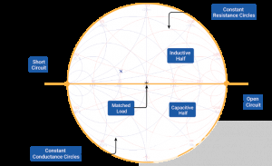
Feeding the complex impedance of the antenna system into SimSmith will result in a point being plotted at the corresponding point on the Smith chart. As shown in the figure above, the complex impedance of an antenna system can be located in either the inductive or capacitive halves of the Smith chart. Matching network components are determined to match the antenna system to the target matching load by utilizing several key points:
Complex impedance points drawn by series inductor moving clockwise along a constant resistance circle
Complex impedance points drawn by series capacitors moving in a counterclockwise direction along a circle of constant resistance
Complex impedance points drawn by parallel inductors moving counterclockwise along a constant circle
Complex impedance points plotted by parallel capacitors moving clockwise along a constant conductance circle
Multiple components or combinations of components may be required in series or parallel configurations to match target impedance
It is best to use a series inductor and a shunt capacitor because increasing the component values of both will cause the plotted impedance point to move further along the locus of the constant resistance/conductance circle. This is advantageous because extremely low values of inductance or capacitors are practically impossible to achieve
Using a single matching network usually results in a drop in system bandwidth, multiple stages of the matching network can be used to achieve proper matching and optimal bandwidth
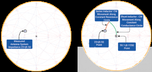
For example, the figure below shows the matching of an antenna system with a complex impedance of 25+j8.5Ω to a target impedance of 50Ω using a series inductor and parallel capacitor.
Although impedance matching may seem complicated, it ensures the best performance of any wireless product where the antenna might otherwise become a bottleneck in product performance.


