
FM transmitter circuit diagram Daquan (FM radio / FM intermediate frequency / megawatt radio transmitter circuit diagram detailed explanation)
Description
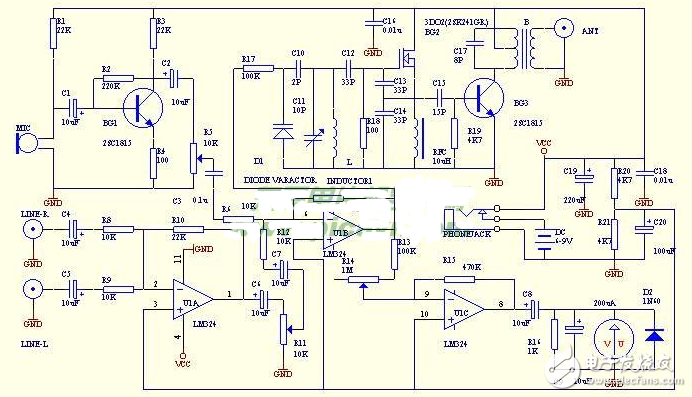
Frequency modulation (FM) transmitter circuit diagram (1)
The working principle and circuit diagram of the FM transmitter meet the requirements of the transmission distance, and it can also use the microphone and line to input sound signals at the same time for background dubbing. The circuit also adds a modulation monitoring meter to better grasp and use the transmitter. The circuit is shown in the figure below. After reading the brief introduction, do you think it has as many functions as a set of radio station equipment? Yes, this small transmitter can help you easily set up an amateur FM radio station! The coverage is around 500M.

Circuit principle and component selection:
After the microphone picks up the signal, it is coupled into the voltage negative feedback single-tube amplifier composed of BG1 and peripheral circuits through C1, and the weak voltage signal is amplified to a sufficient amplitude and enters U1B together with the amplified line input signal of U1A for mixing. The mixed signal is modulated by R17 all the way to the quizbi LC oscillator composed of BG2 field effect transistor and surrounding circuits. High stability. The waveform is good and the modulation bandwidth is particularly important for amateur production of FM transmitters. Finally, the post-stage amplifier cast by BG3 is amplified and transmitted through the transmitting antenna, and the broadcast can be listened to with an ordinary FM radio. The other signal is amplified by the amplifier composed of U1C and then rectified by D2 to drive the microammeter with DC to closely monitor the modulation amplitude of the signal. It is advisable that the modulation degree should not exceed 85% when used. The integrated circuit adopts LM324 and other general-purpose four-operation amplifiers, and forms a single power supply reverse input working mode, that is, the voltage of the positive phase input terminal is set at half of the power supply voltage. The monitor head is 200u type, and BG1 and BG3 use 2SC1815. BG2 uses 3DO2 field effect transistor, and D2 varactor diode uses 1S2267. The antenna is required to use 1/4 wavelength, such as using a whip antenna, it is best not to be less than one meter. Otherwise, the overdue launch effect will not be achieved.
Frequency modulation (FM) transmitter circuit diagram (2)
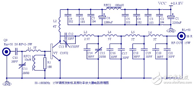
Classical 15W FM Transmitter Circuit Diagram
Frequency modulation (FM) transmitter circuit diagram (3)
The circuit design of the wireless microphone is reasonable, the shape is beautiful and generous, the sound transmission distance is long, the service life is long, the cost is affordable, and the power consumption is small, which is very suitable for receiving and using ordinary FM radio.
Production of the oscillating coil L: use a Ф0.5mm enameled wire to flat-wound 4T on a Ф5mm straight shank drill and take it off.
Adjustment of the oscillating coil L: Turn on the radio (placed in the FM segment) and the microphone switch, then hold the microphone, and adjust the radio knob while speaking into the microphone until your own voice comes out from the radio. If you still can’t hear your own voice in the whole frequency band (ie 88~108MHz), carefully move the vibrating coil L, and only need to open or reduce the distance between each turn of the coil, and you should be careful when adjusting. If adjusting the tightness of the coil still has no effect, solder off L to add one turn or reduce it by one turn (due to the influence of electronic component parameters), and continue the above adjustment after re-soldering.

Before preparing for installation and production, please use a multimeter to screen the quality of each component. If possible, measure the capacitance of each ceramic capacitor, so that it will be foolproof and the installation will be successful. The quality must be ensured during welding, and false welding, false welding and wrong welding should not occur.
Frequency modulation (FM) transmitter circuit diagram (4)
The figure below is the circuit diagram of the FM receiving device where the voice transmitter uses the FM signal carrier to transmit the voice signal.
Parts List:
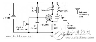
R1=4.7K
R2=330 ohms
C1=0.001uf (1NF)
C2=10-40pf
C3=4.7pf
Q1=2N3904
L1=see text
Miscellaneous = electret mic, antenna, 3V battery (battery)
Circuit configuration:
It’s a lot easier to build tiny transmitters, using a minimum of parts. Construction is straightforward and non-critical. Although this design uses a 3 volt power source (such as a lithium coin or button cell), a 9 volt battery can be utilized instead, increasing the value of R1 and R2 to 1K. C4 is an optional RF bypass capacitor that can help improve performance and range a bit. Experiments found that the best results.
L1 is produced by stripping the insulation of the 22 meter connection wire, then wrapping it in the threaded groove of a 1/4 diameter bolt, then tightening the bolt from the resulting coil. 8 turns around the resulting bolt. By wrapping the threads, a uniform separation is created between the coil windings.
If you decide to replace the transistor with something similar to what you have, it may be necessary to change or adjust the value of R2R3 to the collector voltage of Q1 (since you changed the transistor, it adjusts this bias at the base of Q1). It should be about 1/2 the supply voltage (about 4 or 5V).
Frequency modulation (FM) transmitter circuit diagram (5)
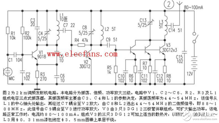
FM transmitter circuit diagram, Figure 2 is the 2KM FM transmitter circuit. This circuit is divided into three stages of oscillation, frequency multiplication and power amplification. In the circuit, V1, C2-C6, R2, R3 and L1 form a capacitive three-point oscillator. The oscillation frequency is mainly determined by the parameters of C3, C4 and L1. The oscillation frequency is 44-54MHZ. The signal is output from the center tap of L1. , and then coupled to V2 for amplification through C7, and the double frequency signal of 44-54 is selected by C8 and L2.
Frequency modulation (FM) transmitter circuit diagram (6)
A very simple FM IF/MW radio receiver circuit design can be designed using the LA1260 Sanyo Semiconductor IC. LA1260IC can be used in AM FM Radio Receiver Electronics Project as you can see in Circuit Schematic. The 1260 integrates many features and functions required for radio receiver applications. Some important functions of LA1260IC: FMIF Amplifier, Quadrature Detector, Auto Focus Preamplifier, Tuning Indicator Driver Output. AM: RF Amplifiers, Mixers, Oscillators (ALC), IF Amplifiers, Detectors, Automatic Gain Control, Tuning Indicator Drivers.
Important features of the main LA1260 FM are: High S/N: FM81dB, AM53dB; low level AMALC MW 130mV SW 70mV to 90mV (7MHz) (24MHz) oscillator; AM whistle jamming AM tuner system whistle 1%, enter in hundred decibels/meter. On-chip LED tuning indicator driver chip for FM/AM selection; separate AM/FM output pins.
Local AM oscillator part, AM local oscillator coil, antenna part circuit and antenna, such as bars, must be separated from each other as much as possible to prevent deterioration of the Q value. Pin 16 (AM oscillating injection needle) and pin 14 (RF input pin) must be separated from each other. The recommended power supply for this radio receiver circuit is 4.5 VDC, but the LA1260IC accepts input voltages ranging from 3 to 8 VDC.


